MIT Unveils Game-Changing Chip Design, Boosting AI Hardware to Supercomputer Speeds
January 5, 2025
A groundbreaking research led by Jeehwan Kim, an associate professor at MIT, has been published in the journal Nature, showcasing a new chip design that enhances communication between semiconducting layers.
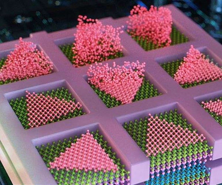
The innovative method allows for the creation of high-performance, multilayered chips without relying on bulky silicon wafer substrates, addressing a significant limitation in the electronics industry.
This new chip design not only improves computing power and capabilities but also enables the fabrication of chips with alternating layers of high-quality semiconducting materials directly on each other.
Researchers successfully grew two types of transition-metal dichalcogenides (TMDs) on top of each other, which are crucial for developing n-type and p-type transistors.
Inspired by metallurgy, the technique allows for the growth of single-crystalline materials at temperatures below 400 degrees Celsius, preserving the integrity of underlying circuitry.
Kiseok Kim, the first author of the study, highlighted that their growth-based method overcomes traditional limitations of 3D chip fabrication, particularly issues related to vertical alignment and yield.
This approach paves the way for creating AI hardware capable of rivaling the speed and storage capacity of today's supercomputers.
In 2023, Kim's group had previously developed a technique to grow high-quality semiconducting materials on amorphous surfaces, which is suitable for smaller, high-performance transistors.
To further commercialize their innovation, Kim has founded a company called FS2 (Future Semiconductor 2D materials) aimed at advancing the development of stackable chips.
As the electronics industry grapples with limitations on the number of transistors that can fit on a single chip, manufacturers are increasingly exploring multilayered chip designs.
This new method could potentially double the density of semiconducting elements in chips, leading to significant advancements in both logic and memory applications.
Summary based on 1 source
Get a daily email with more Tech stories
Source

Space Daily
MIT engineers grow